SPI Supplies Brand Silicon Chip Substrates
| Size | 5x5mm x 525um |
|---|---|
| Item | 4136SC-AB |
| Availability | In Stock |
| Size | 5x7mm x 525um |
|---|---|
| Item | 4137SC-AB |
| Availability | In Stock |
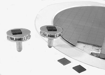
4136SC-AB 5x5mm x 525um – 270 Chips/wafer
4137SC-AB 5x7mm x 525um – 187 Chips/wafer
4 inch (100 mm) diameter wafer
- Orientation: <100>·
- Resistance: 1-30 Ohms
- Type: P (Boron)
- Wafer thickness: 18-21 mil (460-530µm)
- Roughness: 2nm, polished on one side
SPI Supplies Silicon Chip Specimen Substrates are cut from electronics industry grade <100> wafers. They are highly polished with a smoothness comparable to a glass cover slip. Excellent as substrates for SEM and SPM applications, the silicon chip substrates are opaque and exhibit low electrical resistivity, essentially rendering them "conductive" in the SEM where micro amps are involved in terms of currents. They are chemically inert and can be further cleaning prior to use without concern about chemical etching effects occurring. They can also be heated without changes occurring to temperatures far higher than glass, making certain heating experiments possible that would otherwise be impossible with glass.
PACKAGING:
An entire 100 mm (4") wafer is pre-cut to a depth that individual squares (e.g. chips) can easily be broken off when needed for use. Occasionally one or two of the chips might not break off cleanly so the number guaranteed per wafer is slightly less than the theoretical number.
APPLICATIONS
Materials Science:
Use when colloidal size nanoparticles are being studied at high resolution as in a FESEM. The silicon has the smoothness of a glass cover slip yet has the needed conductivity for high-resolution SEM examination. Because the silicon substrate is somewhat conductive, one can lessen the need for metal coating, which can easily cover up features that might otherwise be resolved. Should metallization still be needed, perhaps for contrast considerations, we recommend using the Osmium Plasma Coater line of osmium metal coaters offered through SPI Supplies.
Life science samples:
This is an ideal substrate for the growing and/or mounting of cells since the surface smoothness is comparable to that found on a glass cover slip or microscope slide. And because it is silicon and not glass, one need not worry about their important specimens suffering the fate of glass corrosion. Another feature of the silicon chip substrates is that they can be processed and critical point dried exactly as if one were using glass cover slips. And because of the inertness of silicon, they can also be autoclaved.