Silicon Nitride Membrane Window TEM Grids, 200um thick frames, 75nm thick window,0.5mm window, Low S


| Availability | In Stock |
|---|---|
| Item | 4123SN-BA |
Silicon [CAS #7440-21-3]
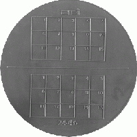
200 µm Thick Frames (Window Size: 0.5 mm)
Packs of 10
Thickness of Membrane Window = 75 nm
The Original Product Line:
These unique membranes of silicon nitride (Si3N4) were made using a highly innovative approach using electronics grade {100} orientation silicon wafers with a a thin film of Si3N4 deposited to the desired thickness. Presently, we have seven different thicknesses of the nitride, 200, 150, 100, 75, 50, 30, and 20 nm.
The next step is to back etch through the silicon wafer to the silicon nitride layer, which produces the "membrane window" effect. While the membranes are very thin and fragile, they are sufficiently "robust" to permit one to conduct their experiments. The product is meant for a single use and we would not recommend trying to clean off old samples for reuse. Distinction between the sides is easy. The membrane side is completely smooth, the back side has the etch pit in it. The "Up" side of the grid is the membrane side, not the etched side.
Details of The Nitride Membrane Material: (ST VS LS Membranes)
This has been an area of some confusion and our goal here is to clarify the precise nature of the SPI membrane window grids. Our original technology produced "stoichiometric" Si3N4 and for the first year or so we offered this particular product line. However, stoichiometric or "ST" membranes had a relatively high residual intrinsic stress which contributed to a less robust film, one that is easily ruptured. With technology advances and additional experience, we have developed the technology to produce "low stress" (LS) silicon nitride membranes. These membranes have a Si:N ratio greater than 3:4, that is, Si is greater than 3. Except for those with membranes 20 nm in thickness all of the SPI silicon nitride are of the low stress variety. The 20 nm are ST.. General information about the electrical resistivity values for these membrane window products can be found here.
Some Suggested Applications for SPI Silicon Nitride Membrane Windows:
Used as an inert substrate at elevated temperatures to observe dynamically, reactions in situ by either TEM or SEM in some instances, by AFM.
Use as a durable (e.g. "robust") substrate for doing "matched pairs" of the same identical area first by TEM and then by SEM.
Use as a durable substrate for matched pairs comparing the AFM vs TEM image.
Use as "wet cells" for both SEM BSE imaging and TEM transmission imaging
Anyone studying nanoparticles will find these membrane window grids to be indispensable for their work. Those studying aerogels and/or xerogels because of the smallness in size of the basic particles, find the SPI silicon nitride membrane window grids especially valuable for their work.
Advantages:
For SEM applications, the background is relatively structureless and featureless (remember, nothing is completely structureless or featureless).
For x-ray microscopy there is really no other way for mounting many of the samples one would want to analyze.
For SEM BSE imaging, cells can be grown directly onto the nitride windows and the volume sealed with a "blank" without membrane for a perfect UHV compatible environmental chamber.
For high temperature applications, we believe that the nitride membranes are stable up to at least 1000°C. A report on information validating the robust nature of the membrane windows can be found here. See a list here of researchers reporting results using the membrane window grids. Morphological information can easily be obtained as a function of annealing time without concern about breakage of the membrane (within limits, of course!).
Are The Membrane Windows Hydrophilic?
The grids, as manufactured tend to be hydrophobic, so if samples are being applied from an aqueous suspension, this can cause suspended nanoparticles to appear in a nonuniform distribution across the membrane. The membranes can be made hydrophilic by treatment in a plasma etcher such as the SPI Plasma Prep II Plasma Etcher, however the effect of the treatment is transitory (I.E. a short period of time). For a fee we can treat the membrane window grids this way, but we can not guarantee the longevity of the effect.
Optical Transparency:
Visually one can "see through" the windows if you view them by transmission light microscopy. There has to be some thickness beyond which the optical transparency starts to decline, but even at 200 nm thickness, they are transparent in the visible range of the spectrum. When considering optical properties, keep in mind that the absorption edge is just below 13 nm. Hence at 13 nm the transmission for a 100 nm membrane is about 44%. At 12.4 nm it drops down to about 13%. Always keep in mind where they are relative to the absorption edge when trying to estimate membrane optical properties. Our target for refraction index is approximately 2.15, but we make no gaurantees nor represent this as a specification of the product.
Flatness and Roughness of The Membrane:
We assume our membranes are as flat as the underlying silicon wafers. In terms of roughness our specification for the starting wafer is to be better than 0.5 nm RMS, but it is not a stated specification for roughness of the final membrane. We have reports of customers doing their own roughness measurements and reporting as good as 0.2 nm RMS. We have not made exhaustive measurements of our own.
In our opinion the flatness is acceptable for most users and similar on both sides. We've never measured the "well" side for flatness because one can not get a SPM probe down into the well. We assume the flatness closely mirrors the that of the underlying silicon wafer. Therefore the well side can't be any more rough than the opposite side, it could only be smoother.
Window Size:
The "standard" window size is 0.5 mm square and this dimension is more than enough for most TEM workers. Remember, larger membrane window is never going to be as robust as a smaller window. We've had some requests for larger windows for TEM and now offer at least two standard products that have a 1 mm square window.
Advis Against Using Larger Membranes for the TEM Grid Application:
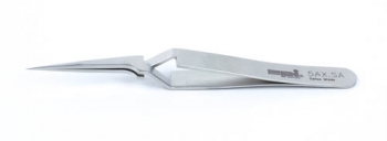
First and most important: The amount of frame left is so little that the grids would "snap" when being broken out of the wafer into individual grids. Secondly: It would be difficult to pick up a grid with such a small frame with a pair of tweezers without damaging the window. We can make larger windows but not in a TEM grid product.
Selection of Window Size:
Those considering larger than the standard (I.E. 0.5 mm) windows generally want a larger field of view. For these we offer the 1 mm window products. For those contemplating processing, smaller windows are desired. All of the SPI Supplies silicon nitride membrane window grid products can be easily spin coated provided arrays of membranes are being coated.
Ultra Thin Membrane Windows:
Our 20 nm windows represent the very latest in production technology for membrane window grids. Remember, the membrane itself is "stoichiometric" and not "low stress" but it does not really matter anyhow since the stress is so low. Any way you look at it, 20 nm is very thin, so thin that we hesitate to guarantee to anyone that the 20 nm windows can be spin coated or exposed to various other forms of processing without rupturing the membrane. The membranes are sufficiently robust to perform as a TEM grid, with the smaller size windows being more robust than the larger ones. We make no guarantee that the 20 nm windows will be completely free of pin-hole defects (for TEM applications, this should not matter).
Silicon Oxide Membrane Windows:
Because of a number of customer requests, we are developing a parallel product line that will have SiO2 instead of Si(Si3N4) membrane windows. The first silicon oxide membrane products in this new family are now available. We also have available perforated silicon oxide membrane window grid.
The silicon oxide membrane window grids will be less stable in some ways to the nitride product. For example, the oxide is compressive so it will be less flat. Also, from a chemical standpoint the nitride is inert to just about everything except free fluorine, but the oxide is reactive to a few different chemical species.
Wet Cell Kits now Available
The SPI Supplies Brand of silicon nitride membrane window grids can be used to create a unique environmental chamber or "wet cells" which permit the BSE imaging of cells and other wet samples at resolutions heretofore just not possible.
Cleaning of Membranes Before Use:
The silicon nitride membrane window grids do not need further cleaning before use. There are occasionally small pieces of nitride scattered around from the snap out corners (that make the frames rounded) but the presence of such debris particles can't be prevented. They should not pose any problems or interference to the user.
If one does want to clean the membranes for some reason, then we suggest using H2 SO4 : H2O2 (1:1) for organic and H2O:HCl: H2O2 (5:3:3) for metals. The membranes are not compatible with ultrasonic treatments. The windows have a tendency to shatter.
Adhesion of Coatings to The Membrane Surface:
All the commonly used coating methods can be used on the membrane but there can be adhesion problems, not necessarily because they are membranes, but just because they are normal surfaces with the properties of normal surfaces. One can use vacuum evaporation, sputter coating, or spin coating without undo problems. In the case of gold coating, we normally apply a thin layer of chromium to enhance adhesion.
Holey Membrane Window Grids
We have also successfully made our first holey membranes using micro fabrication techniques. Such grids make possible the depositing of nanofibers or other samples across the holes so that data can be taken without any contribution from the support being present in the final data. Putting holes into the membrane increases the price typically by 2-3 times, depending on the number of holes needed.
Membrane Windows for Spin Coating:
Sometimes research protocal requires the membrane side to be spin coated, using for example, the widely popular table-top spin coater offered by SPI Supplies, the Model KW-4A. For spin-coating requirements we offer these same membranes in the form of a "multi-frame array". Hence a large number of the membranes can be coated at one time and each frame snapped out individually when needed.